Our technology lab |
Testing |
|
X-ray diffraction |
|
Laser interferometry |
|
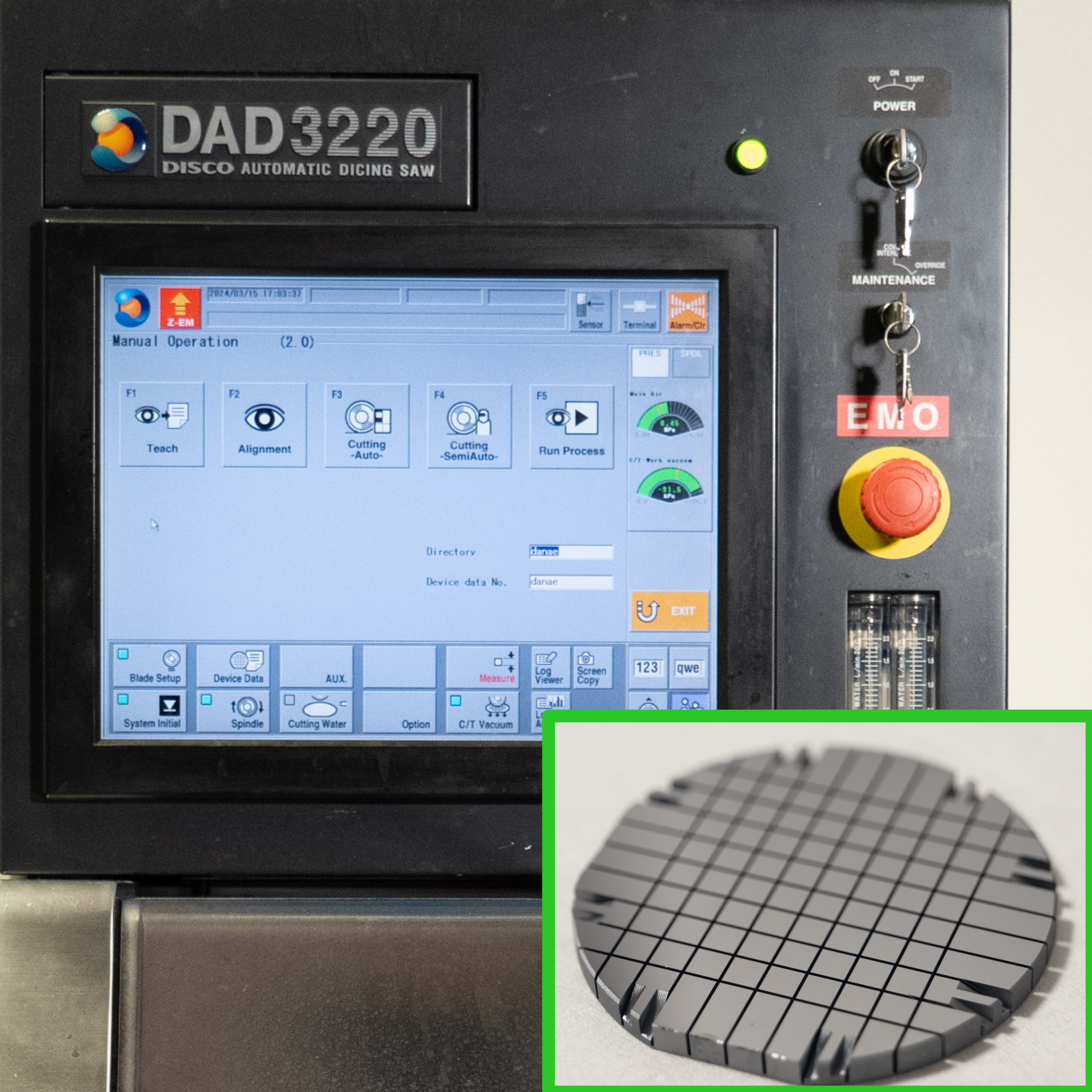
Dicing is a critical process in semiconductor manufacturing, where semiconductor wafers are precisely cut into individual components using diamond blades. This technique is essential for creating integrated circuits and microchips, as it ensures clean, accurate cuts that are crucial for the quality and reliability of the final products. Utilizing equipment like the Disco DAD3220, which offers high precision and efficiency, the dicing process can handle various materials, including silicon, ceramics, and soft metal alloys. The precision of dicing, with positioning accuracy down to microns, is vital for maintaining the performance standards required in semiconductor applications. |
|
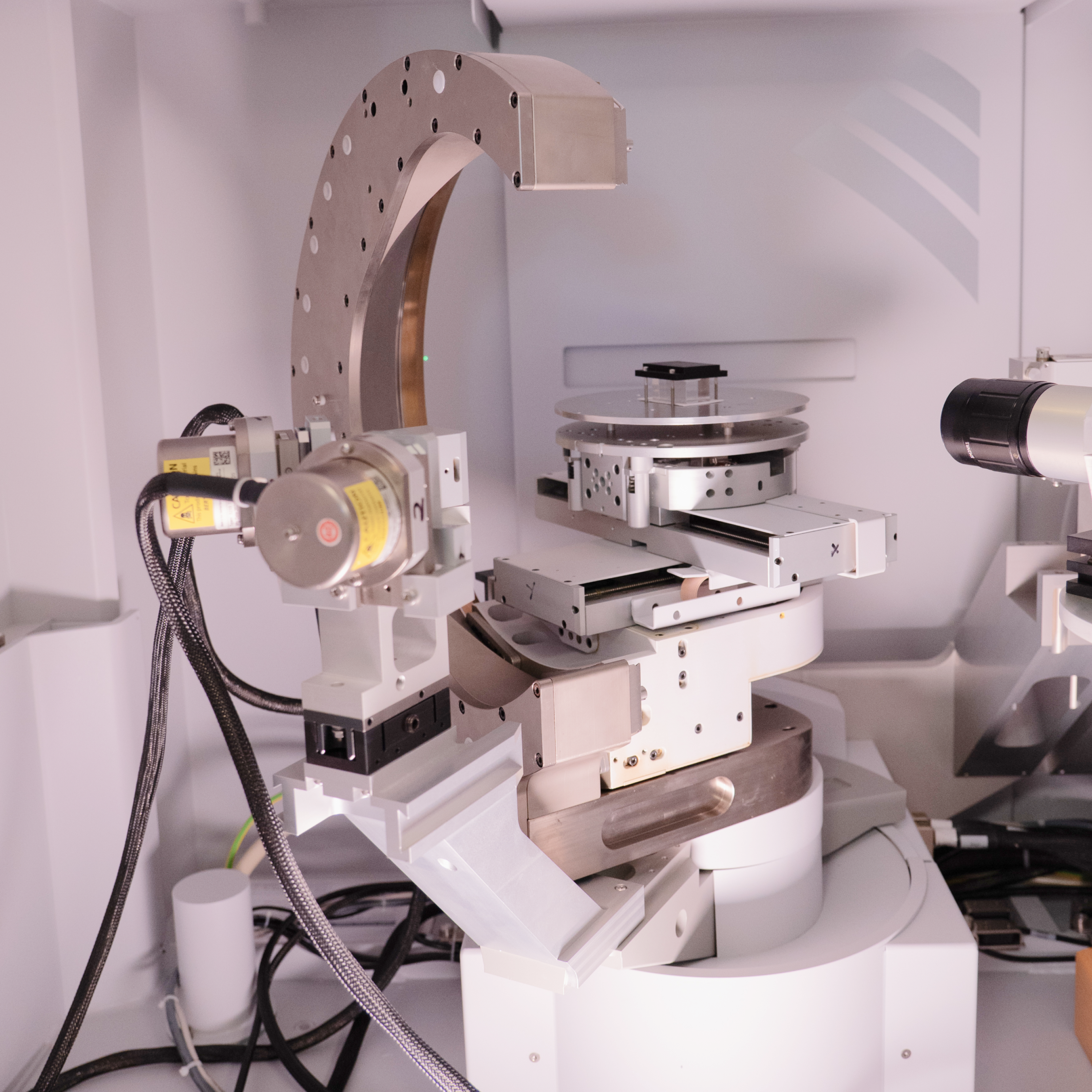
High-Resolution X-ray Diffraction (HRXRD) is instrumental in studying thin films and epitaxial structures, where the arrangement of atoms and defects crucially affects the material's electronic, optical, and mechanical properties. This technique provides detailed insights into crystal orientation, lattice spacing, strain, and defects, aiding in material optimization. Its non-destructive, non-invasive nature allows for in situ analysis during processes such as growth or annealing without altering the sample, making HRXRD invaluable for researchers in materials science and solid-state physics. |
|
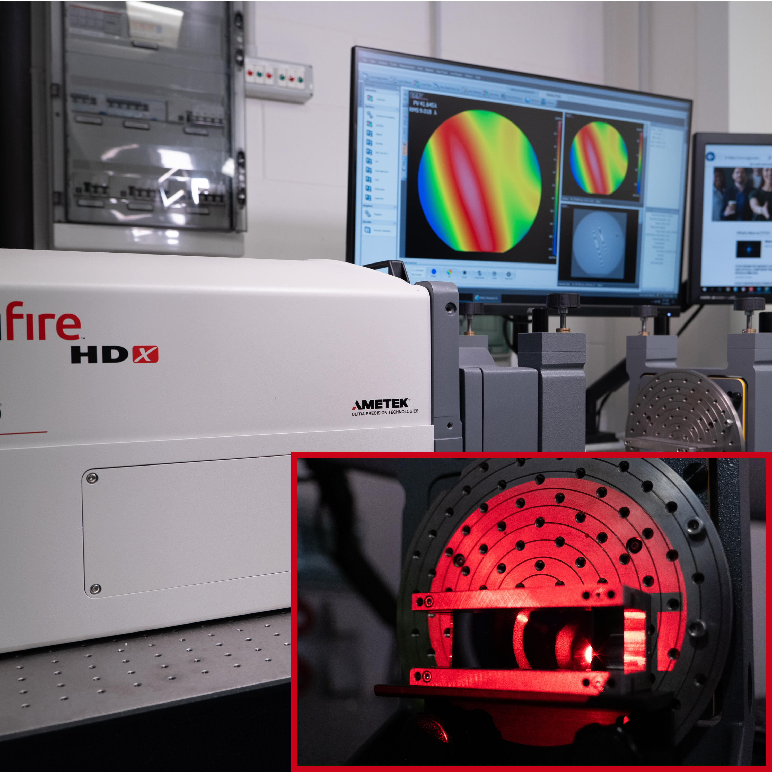
Fizeau laser interferometry is a precise measurement technique utilized in fields like metrology, engineering, and materials science. Named after physicist Armand Fizeau, this method involves splitting a laser beam into two parts: one directed at the object being measured and the other at a reference mirror. The recombined light waves create interference patterns that reveal the surface profile of the object with nanometer-level precision. This non-contact technique is crucial for applications such as semiconductor manufacturing, aerospace engineering, and optics production due to its adaptability and high accuracy. |
Infrared interferometry |
|
Grinding and polishing |
|
Spin coating |
|
Lorem ipsum dolor sit amet, consectetur adipiscing elit. Vestibulum sed enim erat. Sed consequat, libero laoreet cursus porttitor, nulla augue tincidunt magna, sed laoreet nibh nisl in orci. Sed ut felis eget sem viverra interdum. Integer vitae velit id arcu fringilla faucibus. Proin vel augue vel metus porttitor ornare vel et tortor. Donec eu mollis quam, ac mollis dolor. Maecenas aliquet convallis augue, et dignissim odio vehicula eu. Maecenas vestibulum consectetur ullamcorper. Mauris venenatis ante risus. Aliquam feugiat dui eu nulla pharetra semper. Fusce vitae ipsum id lorem consequat sodales a eget purus. |
|
Grinding and polishing are essential for producing high-quality optical and mechanical components, including semiconductors. These techniques refine surfaces of metals, glass, and crystals to achieve precise geometries and finishes. Grinding removes excess material using abrasives, creating a rough surface, while polishing smooths this surface to achieve high accuracy and a mirror-like finish. This combination is crucial in optics for producing flats, mirrors, prisms, and other components, ensuring minimal distortion and aberrations. |
|
Spin coating involves applying a coating solution to a thoroughly cleaned substrate, which is then spun at high speeds (1000 to 8000 RPM) to form a thin, uniform layer. The film thickness is controlled by the solution concentration, spin speed, and duration. This technique is versatile, used for depositing polymers, metals, and ceramics, and is advantageous for its ability to produce uniform films quickly. Despite challenges in controlling thickness and uniformity, spin coating remains a popular choice due to its simplicity, cost-effectiveness, and efficiency. |
Photolitography |
|
Robotic stereolithography |
|
Autocollimators |
|
Photolithography is a process used to pattern features onto a substrate using light. It begins with applying a photosensitive material to the substrate, followed by exposure to UV light through a mask or reticle. The exposed areas harden, forming a pattern that serves as an etch mask for transferring the design onto the substrate. This technique is fundamental in semiconductor manufacturing and other high-precision fields, enabling the creation of intricate patterns and structures with high accuracy. |
|
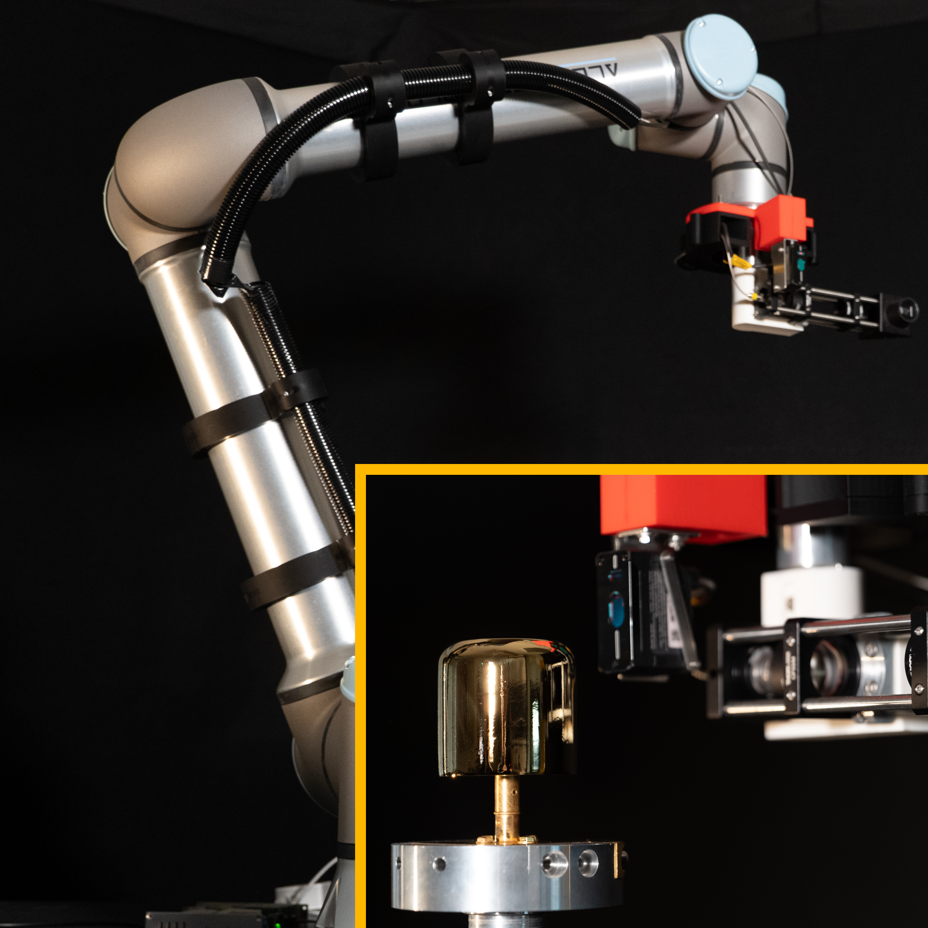
Maskless photolithography utilizes a UV projector or focused laser to selectively expose a UV-sensitive film on a substrate, creating precise patterns without traditional masks. The process involves spinning a coating solution onto the substrate to form a uniform layer, followed by UV light exposure to harden the film in specific areas. This technique, along with collaborative robots (cobots) that handle tasks like wafer positioning, enhances accuracy, speed, and safety in semiconductor manufacturing, though it faces challenges such as UV radiation management and high implementation costs. |
|
An autocollimator is a precision optical instrument designed to measure angular displacements with exceptional accuracy using a rotating mirror. By projecting a laser beam onto a surface and detecting the position of the reflected beam with a photodetector, autocollimators can measure very small angles and calculate the angle between surfaces with high precision. Valued for their simplicity, sensitivity, and accuracy, autocollimators are essential in applications such as aligning optical components, calibrating surveying instruments, and manufacturing precision parts. They are relatively inexpensive, easy to operate, and widely used in various engineering fields. |


